
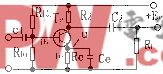
建设电源工程
That may sound like a gloomy assessment, but it reflects the realities of design. DC-DC converters aren't easy. They require extensive component-value calculations and thoughtful selection of the controller IC. They are very sensitive to board layout and component parasitics. And there are few comprehensive sources of design information. Engineering textbooks discuss control theory, loop compensation, and other highly detailed analysis methods. Data sheets for DC-DC converters give specific formulas and some layout information. But little information is available to guide the design of integrated-circuit DC-DC converters from start to finish.
This article provides complete information for a first DC-DC power supply design. It is the result of success and failure by the author on dozens of power-supply designs.
Each topic is covered briefly, and is intended as the launching point for further research.
Device Selection
A proper choice of DC-DC converter IC depends primarily on the design objectives. If the input voltage is always greater than the output voltage, choose a buck-converter topology. If the input voltage is always less than the output voltage, choose a boost configuration. If the input voltage ranges above and below the output voltage, either the buck or boost converter can be used, but it must be adapted to the non-standard input voltage range.In general, output currents below 2A can be accommodated by DC-DC converter ICs with integral power switches. Most modern ICs include MOSFETs as their internal power switches, but some include bipolar transistors. Switches internal to some of the newer ICs can handle up to 5A, and that capability should continue to increase. A device with internal switches is usually a better choice, both for overall simplicity and (often) for lower total cost.
DC-DC converters designed for driving external power switches are usually called controllers. They include drivers capable of delivering up to 2A (briefly) for charging the gate capacitance of external MOSFETs. The ability to quickly charge and discharge a MOSFET gate is critical in achieving high-efficiency conversion, and most DC-DC controllers specify a maximum for the gate capacitance they can drive. (See "MOSFET Gate Capacitance.")
MOSFET Gate Capacitance
MOSFET manufacturers provide many capacitance and switching parameters on their datasheets, but for DC-DC converters, the total gate charge (QG) is of primary interest in most cases. Choose MOSFETs for which QG is within the range recommended by the manufacturer of the DC-DC converter in question. Use the typical value for QG in most cases. The maximum value can be ignored.Another switching parameter of interest is the reverse transfer capacitance (CRSS). CRSS is used in calculating switching loss in the high-side n-Channel MOSFET of a buck converter, per the following equation:
PD(Switching) = (CRSS × VIN(MAX)² × fSW × ILOAD)/IGATE
where IGATE is the peak gate-source current and sink current, and fSW is the switching frequency.
The most popular control scheme is pulse-width modulation (PWM). PWM converters maintain a constant switching frequency over a broad range of loads. That behavior is important, because switching noise from a DC-DC converter can interfere with other processes in a system. Confining the noise to a known band eliminates most of those problems.
The next most common control scheme is pulse-frequency modulation (PFM). Simplicity of implementation made PFM popular with some of the earliest DC-DC converters, and it is still used in some cases. PFM converters excel in applications that require low quiescent current.
The switching frequencies of available DC-DC converters range from 20kHz to over 1MHz. You should avoid devices that operate below 100kHz; such frequencies are typical of old devices with poor efficiency. In general, higher switching frequency allows external components that are smaller in both size and value. (See "High Switching Frequency Reduces Component Size.") If smallest possible size is important in the application, then look for converters with switching frequencies at 1MHz and above. Otherwise, simply choose a device that meets the main criteria specified, and verify that its switching frequency does not interfere with other components in the system.
High Switching Frequency Reduces Component Size
The current trend in DC-DC converters is to higher switching frequencies. The key advantage of higher frequency is smaller component sizes. Inductor values, for instance, are lower. Inductor behavior is governed by the following equations:VL = L (di/dt), WL = (L × i²)/2, and L = N²,
A DC-DC converter transfers energy at a controlled rate from an input source to an output load, and as the switching frequency increases, the time available for this energy transfer decreases. For example, consider a buck converter operating at 500kHz with a 10µH inductor. For most DC-DC converters, changing the frequency to 1MHz allows use of exactly one half the inductance, or 5µH.
Although the inductance value decreases by one half, the current requirement remains the same. The second equation shows that we just reduced the inductor's required energy storage by half as well. In addition, the third equation shows that the number of turns was reduced to 70.7% of the original number. That change lowers the equivalent series resistance (ESR) by the same percentage. So, the resulting inductor has a physical size of approximately half the original, and a lower ESR.
Higher frequency also reduces the size of the output capacitor. In the example above, the capacitance required is 67µF at 500kHz, but only 33µF at 1MHz. The ripple-current specification remains unchanged.
After choosing a particular device type, make the final selection by consulting the databooks or websites of DC-DC converter manufacturers. (See: Power Supply Cookbook, http://www.maxim-ic.com/cookbook/powersupply/.) Avoid using data sheets from databooks, especially if the databook is more than two years old. Always check the manufacturer's website for the latest data sheet. While there, look for application notes that apply to the device you've selected. They serve as a guide, and they often include circuits that are usable with little or no modification. From application notes and data sheets you can obtain the equations that govern the design for your device.
Design Equations
DC-DC converter data sheets should contain equations helpful in designing your particular circuit. If not, consult a textbook or a similar data sheet. Some data sheets list different equations for different modes of operation, so read the IC data sheet carefully to ensure that you've selected proper equations for the required performance and operating mode. Once the major design parameters are known and you have the right equations, the best tool for evaluating the equations is a spreadsheet such as Excel, or an engineering-math program such as MathCAD.Spreadsheet Calculations
Gone are the days when graphs were made by hand. Spreadsheets are now the unsung workhorse for the electrical engineer. They even serve as crude circuit simulators, and their "Solve" feature can eliminate hours of effort in trying to solve a tough equation for a single variable. When used with DC-DC converter equations, the spreadsheet allows an iterative approach that aids component selection by quickly indicating cause and effect relationships.As an example, consider the MAX1742, a buck converter with internal switches. The data sheet's "Design Procedure" section gives necessary information and the order for calculations. We assume a constant +5V input, a +3.3V output with maximum load current of 500mA, and a 500kHz operating frequency.
Use the defined variable names whenever possible. As you enter more equations, define the results of those calculations with more names. Choose the names wisely so you can remember what they mean when you check the calculations later.
First, across the top of a new worksheet enter names for all values predetermined at the beginning of the design procedure (Figure 1). Such names might include VINMIN, VINMAX, VOUT, IOUT, FREQUENCY, and others associated with the converter you select. In the cell immediately beneath the cell containing those names, define a name to match the name typed above it.
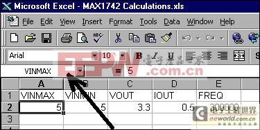
Figure 1. Using cell names in spreadsheets.
To define a cell name: select the cell to be named, pull down the "Insert" menu and select "Name", then select "Define" on the sub-menu. In Excel, a dialog box pops up to suggest (as a default name) the text immediately above the selected cell. To name the cell, click OK on this dialog box. Proceed down the row until all these fields have been named. The foregoing procedure allows you to refer to VINMAX in your calculations instead of cell A2. Note that the selected cell in Figure 1 is A2, with a value of 5. The cell's name is indicated just above the row labeled "A." Next, scan through the design procedure and pick all the required component values (Table 1). Note that original spreadsheet values have been converted to SI units for clarity.
Table 1. Initial Component Calculations
|
|
|
|
|
|
|
|
|
|
|
|
|
First Calculate RTOFF
|
||||
|
|
|
|
|
|
|
|
|
|
|
|
|
Choose the value for LIR, then calculate L and IPEAK
|
||||
|
|
|
|
||
|
|
|
|
||
|
Next the output capacitor parameters are calculated
|
||||
|
|
|
|
||
|
|
|
|
||
|
Soft-start Calculations
|
||||
|
|
|
|||
|
|
|
|||
Component Selection
Using values from Table 1, select the DC-DC converter's peripheral components. Check the data sheet recommendations to ensure each component's suitability for the task. If the calculated inductor value is not available, choose the next smaller standard value available. If a calculated capacitor value is not available, choose the next larger standard size available.The inductor is selected primarily by inductance value and the peak-current requirement. Also make sure that the inductor is designed to operate at the desired switching frequency. If that data is not provided, choose another inductor for which the data is available. Inductors are available in surface-mount and through-hole versions, but in general the surface-mount types offer better performance. In our example, we have a very close match with a Coiltronics Thin-Pac TP1-150, which is a 15µH inductor with 0.73A saturation current.
The input capacitor reduces peak current drawn from the input supply, and reduces radiated noise to other elements of the system. Most data sheets either suggest specific values or give equations for calculating the input capacitor value. Make sure the capacitor is specified with a ripple-current rating near the selected switching frequency. For our 500kHz example, the capacitor could be an organic electrolyte, organic polymer, ceramic, or tantalum type.
Tantalum capacitors can be sensitive to instantaneous voltage changes, so don't use tantalum if the input capacitor is connected to a mechanical switch. Our circuit with its fixed-5V input comes from a regulated supply, so we don't have to worry about that problem. We therefore select a capacitor that meets the ripple-current rating and voltage requirements, such as an AVX TPS series 100µF capacitor in the C size case, rated for 10V and 742mA ripple current.
For loop stability, some DC-DC converters (not the one in this example) require the output capacitor to specify a minimum equivalent series resistance (ESR). If that specification is interpreted as a maximum instead of a minimum, you may lose many hours before finding the error.
The example circuit is designed to operate with a regulated +5V input, so in this case a tantalum capacitor is the best choice. Choose (as a starting point) a capacitor that meets the recommended minimum value of 0.22µF, and verify that it meets the required voltage and capacitance values. For our example, the AVX TPS series 33µF capacitor in the C size case is rated for 10V operation. Its maximum ESR is 0.375Ω, which is close to the target.
The soft-start capacitor and the tOFF resistor have no special requirements, and are selected from the closest available standard values. To complete the component-selection process, choose the remaining values from a typical application circuit.
Spreadsheet Revisited
Because capacitors and inductors come in a finite number of standard values, the closest available value can differ from the calculated value by more than 20%. In that case, the spreadsheet should be recalculated with actual values to verify that the circuit still meets its design objectives. As shown in Table 2, further corrections are not necessary because our RTOFF and inductor choices have a minimal impact on the circuit's operating point.Table 2. Checking actual component values
|
|
|||
|
|
|
|
|
|
|
|
|
|
|
|
|||
|
|
|
|
|
|
|
|
|
|
Component Placement
When laying out the PCB for this example, you should first place the DC-DC converter IC (MAX1742), the inductor, and the input and output capacitors. Then, move those components so the input capacitor is close to the MAX1742's input pins, the inductor is close to the IC's LX pin, and the output capacitor is close to the inductor and the IC's ground pins. Seldom are all these criteria compatible with one another, and often one of the component locations must be compromised to optimize another.The most critical node in most cases is the common ground between the input and output capacitors and the ground pin of the IC. These three grounds must be very close, usually within 10mm of one another (Figure 2a-2b). During the charge cycle (Figure 2a), current flows from the input capacitor through the high-side switch, through the inductor, through the output capacitor, across the ground plane, and back into the input capacitor. During the discharge cycle (Figure 2b) current continues to flow through the inductor, through the output capacitor, across the ground plane, back through the IC's ground pin, through the low-side switch, and back into the inductor.
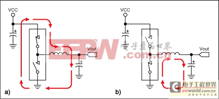
Figure 2. These diagrams illustrate current paths during the charge (a) and discharge (b) cycles.
Because this circulating current can interfere with other circuits, its path length must be kept short. (Short paths also contribute to stable operation and good efficiency.) Too long a path length in the ground portion (during either cycle) can compromise the 0V reference for other circuit elements. That condition can also lead to poor regulation, excessive output ripple, and even loss of function. Placing the input capacitor ground, output capacitor ground, and IC ground adjacent to each other minimizes those unwanted effects.
The next most important connection, the junction between the inductor and the output capacitor, keeps the regulator's output impedance low. The remaining two connections are of equal sensitivity, and one or the other may be somewhat compromised; either by longer traces to circumnavigate other PCB elements, or by vias in the conductor path.
Power Ground
After placing components according to the criteria above, the common ground is connected, either with wide traces or with a polygon of solid copper. Use as much copper as possible to create a low-impedance path between the elements.Local Ground
The typical application circuit for many DC-DC converter ICs indicates multiple symbols for ground, which is an excellent hint on how to accomplish a successful circuit layout. One of the different symbols often indicates a local ground plane. Elements that connect to the local ground plane can include reference-bypass capacitors, resistor dividers, and resistors that set operating points (such as resistor RTOFF in the example).The local ground plane is also a solid copper polygon, usually connected to the power ground plane at one point only; typically the pin titled PGND. Local ground planes prevent switching currents from polluting the low-noise local ground plane. Such currents often exceed 10A.
Ground Plane
Because many systems rely on a separate ground plane for all components on the PCB, it is often tempting to use the ground plane of the DC-DC converter section for that purpose. Such an option should be avoided in all cases. The switching currents mentioned above can cause catastrophic ground glitches across the board, producing excessive EMI, causing invalid logic states, and raising the noise floor. The proper interface between DC-DC converter circuitry and the ground plane is a single via (or a small grouping of multiple vias), leading from the poured copper power ground to the buried ground plane.Signal Routing
After completing the initial ground layout, make the required connections for the first four critical components and then place and route the remaining components. A useful approach is to take all non-critical signals to the backside of the PCB with small vias, reserving the top side of the board for the routing of critical traces.Many approaches are available for signal routing on circuit boards. An easy way is to consider the DC and AC components of a signal, and route accordingly. Remember that every wire is a resistor and an inductor as well. Each signal must be considered with regard to its use in the circuit to determine optimal trace width and length. High-speed and high-current signals demand short, wide routing traces. Longer, thinner traces are appropriate for non-critical signals such as low-speed logic.
Verification
After the converter is completed, the boards manufactured, and the components assembled, the overall design should be verified for performance to the original criteria. If the design was implemented diligently with regard to the issues discussed above, the chances for initial success are good. But, even the best power supply designers must often tweak their designs, and sometimes repeat the whole process when they uncover new issues or ones previously unconsidered.Efficiency
Efficiency can be a key performance parameter. That is usually the case for devices operating from a battery, and is especially true for power supplies in laptop computers. Power supply efficiency in laptop computers affects battery life, but it also contributes power dissipation, and it should be coordinated with the heat-removal limitations. Note that a converter supplying 50W at 85% efficiency dissipates 7.5W inside the computer case.In laptops, the efficiency is important over a wide range of operating conditions. Examples include low battery, full battery, and battery charging, under both standby and operating states. In other applications, the efficiency-critical points depend on how the device is used. Light-load efficiency and quiescent operating current are most important in a pager, while full-load efficiency and heat generation are most critical in network hardware.
Load Regulation
A converter's ability to stay within the specified output-voltage tolerance regardless of load is called load regulation. It applies at DC, but it also includes fast transients such as those encountered with Intel Speed-Step™ processors. You should verify that the output voltage stays within specification when loaded with currents ranging from zero to the maximum. Ensure that the output voltage does not undershoot its minimum value when the load changes quickly from minimum to maximum, and also ensure that the output voltage does not exceed its maximum value when the load current goes from maximum to minimum.Line Regulation
The converter's ability to maintain output-voltage regulation with a varying input voltage is called line regulation. Again, it should be examined both at DC and with a fast AC transient. An AC transient is encountered when a laptop computer switches from its wall supply to it internal battery, and when it switches back from battery to the wall supply. In some systems, the voltage change can be as large as 10V. Verify that the output voltage stays within specification when the input voltage changes from minimum to maximum, and make sure that step changes in the input voltage do not cause peaks or valleys in the output voltage that exceed the output-voltage specifications.Temperature Sensitivity
Often, a system is evaluated in a lab setup and then deemed ready for prime time. But, a critical condition that needs further examination is operation over the worst-case operating-temperature range. Performance to the electrical criteria above should be recorded for comparison at the highest and lowest temperatures the system will encounter during operation. Watch for parameters that change drastically, and those that approach upper or lower limits over temperature.The best way to evaluate a system over temperature is to use an environmental chamber. The chamber lets you conduct computer-controlled experiments over a broad range of temperature, and with an accuracy of 1°C or better. Because most people don't have a chamber handy, however, they must make do with less sophisticated equipment. Common heat guns and even hairdryers are useful in heating a circuit while under test. To cool a circuit well below ambient temperature, spray it with a compressed inert gas called cold spray (offered in many technical catalogs).


评论