
TI ADS528x 8路ADC解决方案
TI 公司的ADS528x是 8路高性能低功耗模数转换器(ADC),具有LVDS输出和各种可编程的特性,非常适合各种高度定制化的应用,并提供非常好的系统集成度。
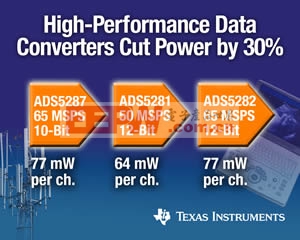
本文引用地址://m.amcfsurvey.com/article/198984.htmADS528x的功耗比同类产品低30%,最高取样速率65 MSPS 的每路功耗仅为77 mW。ADS528x广泛应用在无线基站,医疗设备和测试仪表中。本文介绍了ADS528x的主要性能,功能方框图和模拟输入电路模型图。
The ADS528x is a family of high-performance, low-power, octal channel analog-to-digital converters (ADCs). Available in either a 9mm × 9mm QFN package or an HTQFP-80 package, with serialized low-voltage differential signaling (LVDS) outputs and a wide variety of programmable features, the ADS528x is highly customizable for a diversity of applications and offers an unprecedented level of system integration. An application note, XAPP774 (available at
主要特性:
·Speed and Resolution Grades:
·ADS5281: 12-bit, 50MSPS
·ADS5282: 12-bit, 65MSPS
·Power Dissipation:
·48mW/Channel at 30MSPS
·55mW/Channel at 40MSPS
·64mW/Channel at 50MSPS
·77mW/Channel at 65MSPS
·70dBFS SNR at 10MHz IF
·Analog Input Full-Scale Range: 2VPP
·Low-Frequency Noise Suppression Mode
·6dB Overload Recovery In One Clock
·External and Internal (Trimmed) Reference
·3.3V Analog Supply, 1.8V Digital Supply
·Single-Ended or Differential Clock:
·Clock Duty Cycle Correction Circuit (DCC)
·Programmable Digital Gain: 0dB to 12dB
·Serialized DDR LVDS Output
·Programmable LVDS Current Drive, Internal Termination
·Test Patterns for Enabling Output Capture
·Straight Offset Binary or Twos Complement Output
·Package Options:
·9mm × 9mm QFN-64
· HTQFP-80 PowerPAD Compatible with ADS527x Family
应用:
·Medical Imaging
·Wireless Base-Station Infrastructure
·Test and Measurement Instrumentation
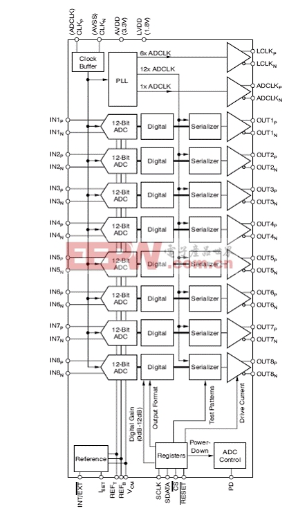
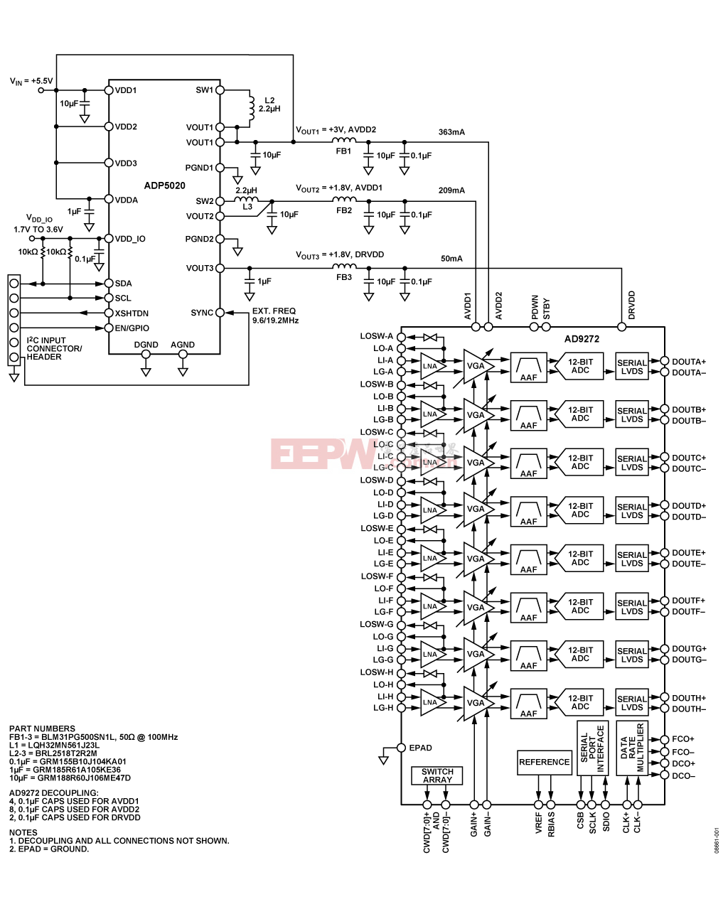
图1 ADS528x 功能方框图
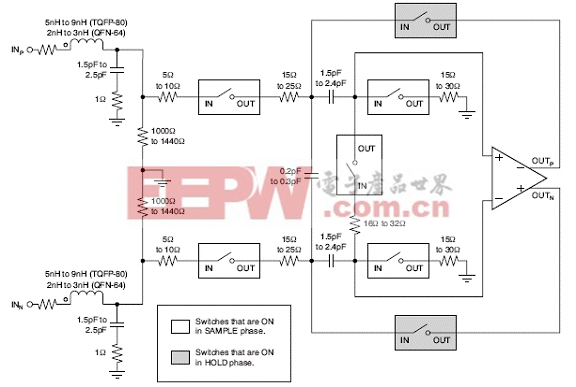
图2 ADS528x 模拟输入电路模型
更多医疗电子信息请关注:21ic医疗电子频道

模数转换器相关文章:模数转换器工作原理


评论