
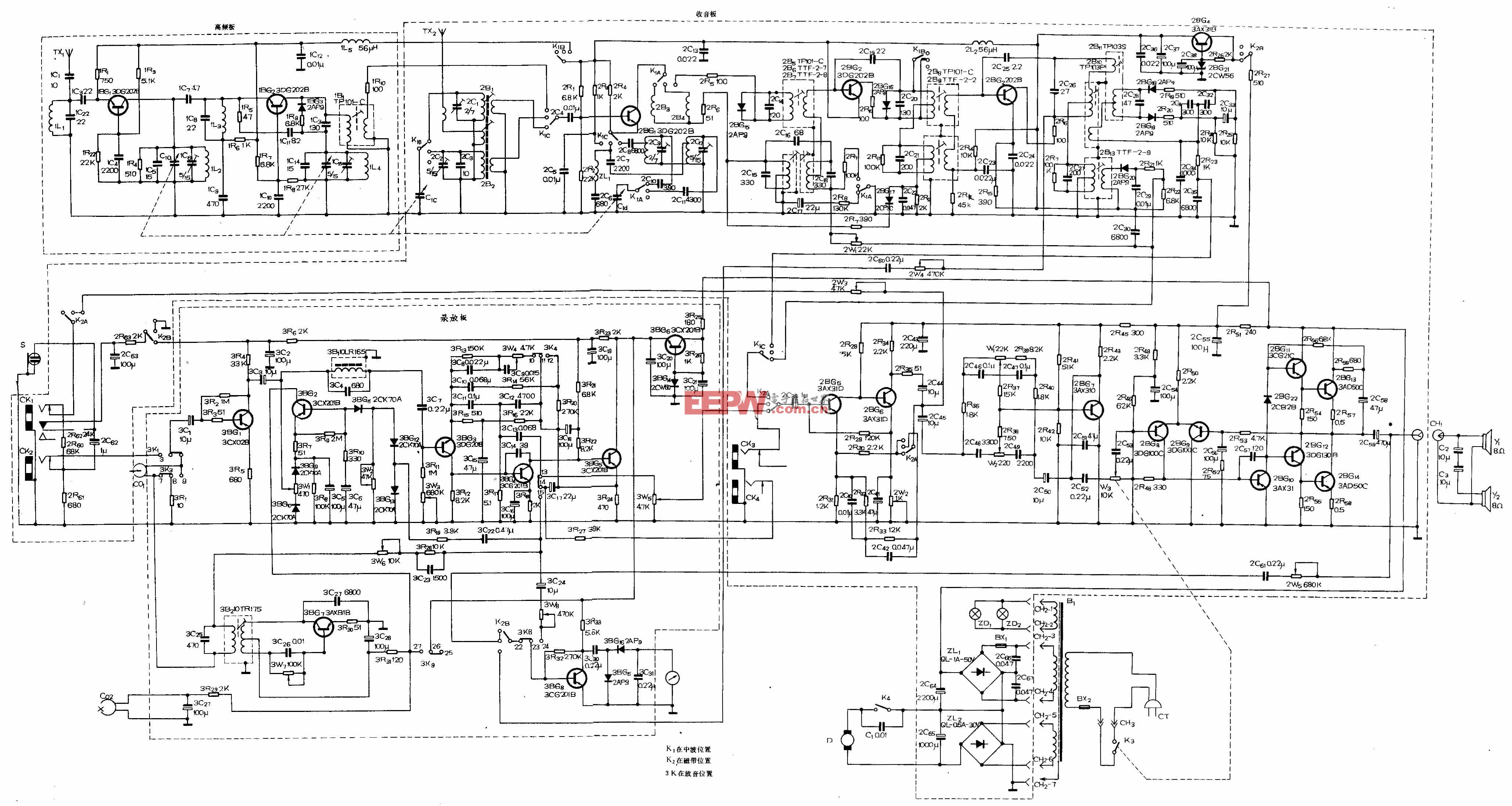
IMEC将在SPIE会议上发布下一代半导体微光刻研究进展
IMEC将于2月23日至27日在美国加州San Jose举行的SPIE先进微光刻会议上展现半导体光刻研究中最新的研发突破。
本文引用地址://m.amcfsurvey.com/article/91433.htmIMEC将在会上发表26片论文。这些论文报道了IMEC及其世界领先的EUV和双版光刻技术合作伙伴在32nm以下节点光刻技术中所获得的成果。光刻技术的一系列挑战都在这些论文中有所涉及,包括材料、制造工艺、测量、检测、工艺控制、微光刻、可制造设计和可选择光刻技术等。
IMEC's record 26 paper presentations to show SPIE attendees the newest advances in next-generation semiconductor microlithography
LEUVEN, BELGIUM - FEBRUARY 18, 2009 - IMEC technologists will present their newest breakthroughs in advanced semiconductor lithography research and development at next week's SPIE (www.spie.org) Advanced Microlithography Conference, to be held February 23 - 27 in San Jose, California.
IMEC will present a record 26 papers at the conference. The papers report progress realized by IMEC and its world-leading core partners on EUV and double patterning lithography targeting the sub-32nm node. The range of lithography challenges are covered, including materials, manufacturing process technology, metrology, inspection, process control, optical microlithography, design for manufacturing, and alternative lithographic processes.
"Stimulated by these record number of papers and with a concerted effort from all actors involved in double patterning and EUV lithography research, IMEC is determined to advance cost-effective double patterning towards the 32nm node and EUV full speed towards the (sub-)22nm node", stated Kurt Ronse, Advanced Lithography Program Director of IMEC. "SPIE provides the prestigious forum for the industry's technologists to share findings and move semiconductor manufacturing forward to accomplish this common service.
Kurt Ronse continued, "As technologists, our goal is to enable engineers and scientists to see their IC designs become reality through manufacturing. Through IMEC's collaborative research, we have achieved many milestones to discuss with our international colleagues."
IMEC's papers are as follows:
Advances in Resist Materials and Processing Technology XXVI
1. EUV resist requirements, absorbance and acid yield, Roel Gronheid, IMEC (Belgium); Carlos Fonseca, Tokyo Electron America, Inc. (United States); Michael J. Leeson, Intel Corp. (United States); Jacob R. Adams, Jeffrey R. Strahan, C. Grant Willson, The Univ. of Texas at Austin (United States); Bruce W. Smith, Rochester Institute of Technology (United States)
2. Newly developed positive-tone resists for Posi/Posi double patterning, Tsuyoshi Nakamura, Masaru Takeshita, Satoshi Maemori, Tokyo Ohka Kogyo Co., Ltd. (Japan); Ryusuke Uchida, Tokyo Ohka Kogyo America, Inc. (United States); Ryoichi Takasu, IMEC (Belgium); Katsumi Ohmori, Tokyo Ohka Kogyo Co., Ltd. (Japan)
3. Analysis of the effect of point-of-use filtration on microbridging defectivity, Jennifer Braggin, Entegris, Inc. (United States); Roel Gronheid, Shaunee Y. Cheng, Dieter Van Den Heuvel, Sophie Bernard, Philippe Foubert, IMEC (Belgium); Craig A. Rosslee, SOKUDO USA, LLC (United States)
4. Integration of improved develop process for topcoat-less immersion resists, Craig A. Rosslee, SOKUDO USA, LLC (United States); Philippe J. Leray, David Laidler, IMEC (Belgium); Masahiko Harumoto, Akihiro Hisai, Michio Tanaka, SOKUDO Co., Ltd. (Japan); Glen Mori, SOKUDO USA, LLC (United States)
5. EUV resist requirements: absorbance and acid yield, Roel Gronheid, IMEC (Belgium); Carlos Fonseca, Tokyo Electron America, Inc. (United States); Michael J. Leeson, Intel Corp. (United States); Jacob R. Adams, Jeffrey R. Strahan, C. Grant Willson, The Univ. of Texas at Austin (United States); Bruce W. Smith, Rochester Institute of Technology (United States)
6. Fluorinated polymethacrylates as highly sensitive nonchemically amplified e-beam resists, Jeffrey R. Strahan, The Univ. of Texas at Austin (United States); Jacob R. Adams, The Univ. of Texas at Austin (United States) and IMEC (Belgium); Wei-Lun Jen, The Univ. of Texas at Austin (United States); Anja Vanlennhove, NXP Semiconductors (Belgium); Colin C. Neikirk, Timothy Rochelle, The Univ. of Texas at Austin (United States); Roel Gronheid, IMEC (Belgium); C. Grant Willson, The Univ. of Texas at Austin (United States)
7. Calibration of physical resist models: methods, usability, and predictive power, Ulrich K. Klostermann, Thomas Mülders, Denis Ponomarenco, Thomas Schmoeller, Synopsys GmbH (Germany); Jeroen Van de Kerkhove, Peter De Bisschop, IMEC (Belgium).
8. Statistical simulation of photoresists at EUV and ArF, John J. Biafore, Mark D. Smith, KLA-Tencor Texas (United States); Jim W. Thackeray, Rohm and Haas Electronic Materials (United States); Stewart A. Robertson, KLA-Tencor Texas (United States); Roel Gronheid, IMEC (Belgium)
9. Resist fundamentals for resolution, LER, and sensitivity (RLS) performance tradeoffs and the relation to microbridging defects, Benjamin M. Rathsack, Mark H. Somervell, Tokyo Electron America, Inc. (United States); Kathleen R. Nafus, Shinichi Hatakeyama, Tokyo Electron Kyushu Ltd. (Japan); Roel Gronheid, Sophie Bernard, IMEC (Belgium)
Metrology, Inspection, and Process Control for Microlithography XXIII
10. A method to determine dose to target without metrology ambiguity using model-based data analysis, Koen D'havé, Anne-Laure Charley, David Laidler, Shaunee Cheng, IMEC (Belgium)
11. A practical application of Multiple Prameters Profile Characterization (MPPC) using CDSEM on production wafers using Hyper-NA Lithography, Toru Ishimoto, Hitachi High-Technologies Corp. (Belgium); Kohei Sekiguchi, Hitachi High-Technologies Europe GmbH (Germany); Norio Hasegawa, Kenji Watanabe, Hitachi High-Technologies Corp. (Japan); David Laidler, Shaunee Cheng, IMEC (Belgium)
12. Contour-quality assessment for OPC model calibration, Paul S. Filitchkin, John L. Sturtevant, Ir Kusnadi, Thuy Do, Mentor Graphics Corp. (United States); Peter De Bisschop, Jeroen Van de Kerkhove, IMEC (Belgium).
13. Track optimization and control for 32-nm node double patterning and beyond, David Laidler, Philippe Foubert, Philippe J. Leray, Koen D'havé, IMEC (Belgium); Craig A. Rosslee, Len Tedeschi, Glen Mori, SOKUDO USA, LLC (United States)
14. Overlay metrology for double patterning processes, Philippe J. Leray, David Laidler, Shaunee Cheng, IMEC (Belgium); Daniel Kandel, Michael E. Adel, Anat Marchelli, Anna Golotsvan, KLATencor Israel (Israel); Mauro Vasconi, Numonyx Srl (Italy); Bartlomiej W. Salski, QWED (Poland); Berta A. Dinu, KLA-Tencor Israel (Israel)
15. Validation of CD-SEM etching residue evaluation technique for MuGFET structures, Miki Isawa, Maki Tanaka, Tatsuya Maeda, Kenji Watanabe, Hitachi High-Technologies Corp. (Japan); Tom Vandeweyer, Nadine Collarert, Rita Rooyackers, IMEC (Belgium).
16. Diffraction-based overlay metrology: accuracy and performance on multilevel measurements, Mauro Vasconi, Samuele Carrera, Flavio Paleari, Pierluigi Rigolli, Laura Rozzoni, Ermes Severgnini, Numonyx Srl (Italy); Philippe J. Leray, Shaunee Y. Cheng, IMEC (Belgium); Daniel Kandel, Michael E. Adel, Berta A. Dinu, KLA-Tencor Corp. (Israel); Bartlomiej W. Salski, QWED (Poland).
Optical Microlithography XXII
17. Extreme scaling of optical lithography: overview of process integration issues (Keynote), Kurt G. Ronse, IMEC (Belgium)
18. Advances and challenges in dual-tone development process optimization, Carlos Fonseca, Mark H. Somervell, Tokyo Electron America, Inc. (United States); Sophie Bernard, Roel Gronheid, IMEC (Belgium); Steven A. Scheer, Tokyo Electron America, Inc. (United States); Shinichi Hatakeyama, Kathleen R. Nafus, Tokyo ElectronKyushu Ltd. (Japan)
19. Ultimate contact-hole resolution using immersion lithography with line/space imaging, Vincent P. Truffert, Joost P. M. Bekaert, Andy Miller, Mireille Maenhoudt, Alexey Milenin, IMEC (Belgium)
20. Comparison of double-patterning methods using Monte Carlo simulation, Joshua S. Hooge, Tokyo Electron America, Inc. (United States); Kathleen R. Nafus, Shinichi Hatakeyama, Tokyo Electron Kyushu Ltd. (Japan); Shaunee Cheng, Philippe Foubert, Philippe J. Leray, IMEC (Belgium)
21. Modeling laser bandwidth for OPC applications, Christian D. Zuniga, Kostas Adam, Michael Lam, Thuy Do, Mentor Graphics Corp. (United States); Ivan Lalovic, Cymer, Inc. (United States); Peter De Bisschop, IMEC (Belgium)
Alternative Lithographic Technologies
22. Compensation of overlay errors due to mask bending and non-flatness for EUV masks, Manish Chandhok, Sanjay Goyal, Seh-Jin Park, Emily Y. Shu, Guojing Zhang, Marilyn Kamna, Fabian C. Martinez, Intel Corp. (United States); Alan M. Myers, Intel Corp. (Belgium); Gian F. Lorusso, Jan Hermans, Eric Hendrickx, IMEC (Belgium)
23. Stability and imaging of the ASML EUV alpha demo tool, Jan Hermans, Bart Baudemprez, Gian F. Lorusso, Eric Hendrickx, IMEC (Belgium); Andre Van Dijk, ASML Netherlands B.V. (Netherlands); David Laidler, Rik M. Jonckheere, Mieke Goethals, IMEC (Belgium).
24. Measurement and analysis of EUV photoresist related outgassing and contamination, Ivan K. A. Pollentier, IMEC (Belgium); German Aksenov, Katholieke Univ. Leuven (Belgium); Mieke Goethals, Roel Gronheid, Rik M. Jonckheere, IMEC (Belgium); Michael J. Leeson, Intel Corp. (United States)
Design for Manufacturability through Design-Process Integration III
25. Application of pixel-based mask optimization technique for high-transmission attenuated PSM, Kyohei Sakajiri, Alexander Trichkov, Yuri Granik, Mentor Graphics Corp. (United States); Eric Hendrickx, Geert Vandenberghe, IMEC (Belgium)
26. High-precision contouring from SEM image in 32-nm lithography and beyond, John L. Sturtevant, Thuy Do, Ir Kusnadi, Mentor Graphics Corp. (United States); Hiroyuki Shindo, Akiyuki Sugiyama, Hitoshi Komuro, Yutaka Hojo, Ryoichi Matsuoka, Hitachi High-Technologies Corp. (Japan); Peter De Bisschop, Jeroen Van de Kerkhove, IMEC (Belgium)


评论